
Transistors and Op-Amps
Every component so far has been passive. A resistor, a capacitor and a diode can only ever hand on part of what they receive. None of them can make a signal bigger.
This lesson is about the two components that can. The transistor is a switch and an amplifier in one, and it is the component that everything else in electronics is built from. The operational amplifier, or op-amp, is a small block of transistors already wired together and sold as one part, so that you can build an amplifier by adding two resistors.
This is also the last lesson of the analogue half of this course. After this we move to digital electronics, where you will meet the transistor again in a different role.
The Bipolar Transistor
A diode is two layers of doped silicon: one P and one N. Add a third layer and you get a bipolar transistor, also written as BJT (bipolar junction transistor).

There are two ways to stack three layers, and both are used:
- NPN: a thin P layer between two N layers
- PNP: a thin N layer between two P layers
The three connections have names that describe their job:
| Connection | Symbol | What it does |
|---|---|---|
| Emitter | E | emits the charge carriers into the transistor |
| Base | B | the control connection, the middle layer |
| Collector | C | collects the carriers that made it across |
On the symbol the arrow always sits on the emitter, and it tells you the type. On an NPN the arrow points outwards, away from the base. On a PNP it points inwards. The arrow also shows the direction in which the conventional current flows through that terminal.
Which one do I use?
An NPN switches something that sits between the transistor and the plus rail, with the emitter to ground. That is the normal case and the one you will use in the lab. A PNP does the opposite: it sits at the top, between the plus rail and the load. Start with NPN, and use PNP only when the circuit forces you to.
Biasing
Biasing means setting the DC voltages on a component so that it works in the region you want. For a transistor it comes down to what you do with its two junctions: the one between base and emitter, and the one between base and collector.
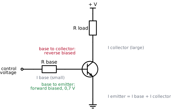
For a normal working NPN:
- The base to emitter junction is forward biased, exactly like a diode. It needs about 0,7 V before anything happens at all.
- The base to collector junction is reverse biased.
Once the base to emitter junction conducts, a small base current starts to flow. And here is the useful part: that small base current allows a much larger collector current to flow. The ratio between the two is the current gain, written as β (beta) or as hFE on a datasheet:
A typical small transistor has a β somewhere between 100 and 300. So 0,1 mA into the base can control 10 mA or more through the collector.
The third current follows from the first two, because everything that goes in must come out:
Three regions
Depending on how much base current you give it, a transistor sits in one of three regions.
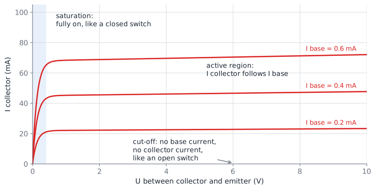
Cut-off. No base current, so no collector current. The transistor behaves like an open switch.
Active region. The collector current follows the base current, multiplied by β. The curves are almost flat, which means the collector current hardly depends on the voltage across the transistor. This is the region you use to amplify.
Saturation. You keep pushing more base current in, but the collector current cannot grow any further because the resistance of the load is now the limit. The voltage across the transistor drops to about 0,2 V. The transistor behaves like a closed switch.
The transistor as a switch
For switching, only two of those three regions matter: cut-off and saturation. That is exactly what a switch is, open or closed, and it is what you will build in the lab.
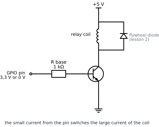
The reason this circuit exists is simple. A microcontroller pin can supply about 10 to 20 mA. A relay coil, a motor or a strip of LEDs needs far more than that. Connect them directly and you destroy the pin. The transistor solves it: the pin only has to deliver the small base current, and the transistor delivers the large load current from the supply.
Example: switching a relay from a GPIO pin
A 5 V relay coil draws 70 mA. You want to switch it from a 3,3 V microcontroller pin, with a transistor whose β is 100.
Step 1: how much base current is needed as a minimum?
Step 2: multiply it, on purpose.
That 0,7 mA would put the transistor exactly on the edge of the active region, where it still drops several volts and gets hot. For switching you want it deep in saturation, so give it about five times more base current than the calculation says:
Step 3: the base resistor.
The base to emitter junction keeps 0,7 V for itself, exactly like a diode, so the resistor gets the rest:
Take 680 Ω, or 1 kΩ if that is what you have. With 1 kΩ the base current is 2,6 mA, which is still nearly four times the minimum.
Step 4: check the heat in the transistor.
In saturation the transistor keeps about 0,2 V:
Nothing. Now compare with a transistor stuck halfway, in the active region, with 2,5 V across it:
Twelve times as much heat, for the same job. That is why a switching transistor is always driven hard into saturation.
Two things this circuit must never be missing
- The base resistor. Without it, the base to emitter junction is a forward biased diode straight across your microcontroller pin. The pin dies.
- The flywheel diode, if the load is a coil. Look back at lesson 2: when the transistor switches off, the coil produces a reverse voltage spike that punches straight through the transistor.
The transistor as an amplifier
Keep the transistor in the middle of its active region instead of slamming it between the two ends, and it becomes an amplifier. A small voltage change on the base produces a large current change in the collector, and a resistor turns that current change back into a large voltage change.
Designing such a stage means choosing resistors that hold the transistor at the right operating point and keep it there when the temperature changes. That is real work, and it is the reason the op-amp exists: someone already did it for you, dozens of transistors at a time, and put the result in an eight pin package.
From here to digital electronics
Notice what the switching part of this section actually said: a transistor is either fully off or fully on, and in between is a region you pass through as quickly as possible.
That is the whole idea behind digital electronics. Off is 0, on is 1. Put a few transistors together and you get a gate that performs logic. Put a few thousand gates together and you get a processor. The chip in your Raspberry Pi contains billions of transistors doing nothing more exciting than what you just calculated: switching on and off.
The rest of the analogue world is about the region in between. The digital world, which is where this course goes next, is about avoiding it.
Try it yourself!
Question 1: A transistor with β = 200 has a base current of 0,05 mA. How much collector current can flow?
Solution
Question 2: You switch a 120 mA load with a transistor whose β is 100, from a 5 V pin. Which base resistor do you choose?
Solution
Minimum base current:
Five times over, to be safely in saturation: mA.
The Operational Amplifier
An operational amplifier is a complete amplifier in one component: a few dozen transistors, already wired together, with the connections you need brought out to pins. It has two inputs and one output, and it does one thing:
It looks at the difference between its two inputs and multiplies that difference by an enormous number.
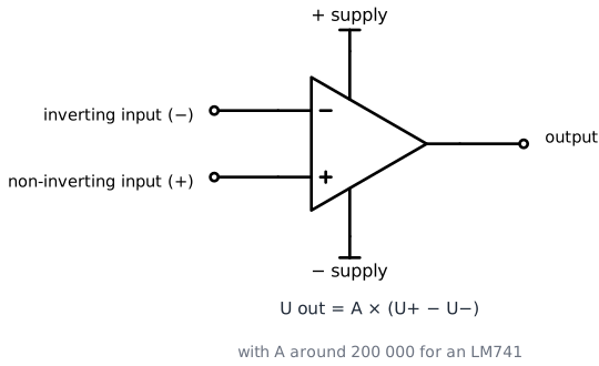
The two inputs have names that come straight from that formula:
- The non-inverting input (+): when this one goes up, the output goes up.
- The inverting input (−): when this one goes up, the output goes down.
The multiplier A is the open loop gain, and for the classic LM741 it is about 200 000. That number is so large that it is almost useless on its own, as you will see in a moment, and taming it is what the rest of this lesson is about.
The LM741
The LM741 dates from 1968 and is still the op-amp you meet first, because it is cheap, hard to destroy and behaves exactly like the theory says.

Of the eight pins you use four in practice: the two inputs, the output, and the two supply pins. Pins 1 and 5 (offset null) and pin 8 (not connected) stay empty in everything you build in this course.
An op-amp needs a positive and a negative supply
If the output has to be able to go below 0 V, the chip needs a supply below 0 V. That is why an op-amp is normally powered from a dual supply, for example +12 V and −12 V, with the ground in the middle.
You can make one from the two channels of your bench supply: set both to 12 V, connect the − of channel 1 to the + of channel 2, and call that middle point your ground. The + of channel 1 is then +12 V and the − of channel 2 is −12 V.
The ideal op-amp against the real one
Almost every calculation in this lesson assumes an ideal op-amp. That is not laziness: the real component is close enough that the difference does not matter, as long as you know where the limits are.
| Property | Ideal | LM741 |
|---|---|---|
| Open loop gain | infinite | about 200 000 |
| Input current | zero | about 80 nA |
| Input resistance | infinite | about 2 MΩ |
| Output resistance | zero | about 75 Ω |
| Bandwidth | infinite | see below |
| Output swing | up to the supply | about 1,5 V short of each supply |
That last line matters in practice: on a ±12 V supply an LM741 output reaches roughly +10,5 V and −10,5 V, not the full ±12 V. Modern rail to rail op-amps do get within millivolts of their supply.
Open loop frequency response
The gain of 200 000 only exists at DC and at very low frequencies. From about 10 Hz upwards it falls, at exactly the 20 dB per decade you learned about with filters.

The line crosses a gain of 1 at about 1 MHz. That number is the gain bandwidth product, and it is the most useful specification on the whole datasheet, because it stays constant:
So you get to choose one of the two, not both:
| You ask for a gain of | You get a bandwidth of |
|---|---|
| 1 | 1 MHz |
| 10 | 100 kHz |
| 100 | 10 kHz |
| 1000 | 1 kHz |
An LM741 with a gain of 1000 is useless for audio, because it gives up at 1 kHz. If you need both gain and bandwidth, you use two stages of ten instead of one stage of a hundred, or you buy a faster op-amp.
Switching characteristics
There is a second limit, and it has nothing to do with the gain. The output of an op-amp cannot jump. It can only move at a certain maximum speed, called the slew rate, measured in volts per microsecond.
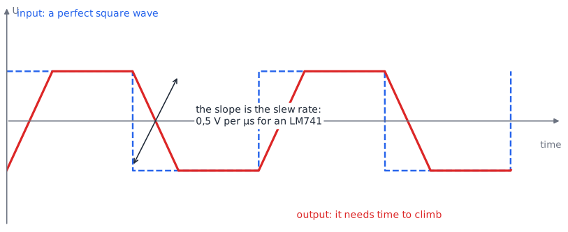
For an LM741 the slew rate is 0,5 V/µs. So to swing the output from −5 V to +5 V, a jump of 10 V, it needs:
Feed that op-amp a 10 V square wave at 25 kHz and each half period lasts 20 µs, so the output spends the entire time climbing. What comes out is not a square wave at all, it is a triangle.
This is why fast comparators and audio power stages use op-amps with slew rates of tens or hundreds of volts per microsecond. For a slow sensor signal, 0,5 V/µs is plenty.
Feedback: taming the gain
Take the formula literally for a moment. With a gain of 200 000 on a ±12 V supply, an input difference of just 0,06 mV already drives the output to its limit. Any real signal would push the output straight against one of the supply rails and keep it there. As an amplifier, that is worthless.
The fix is negative feedback: you take a part of the output and feed it back to the inverting input. The op-amp then works against itself, and the circuit settles into a stable state. From that one idea follow the two rules that let you analyse every circuit in this lesson without any maths beyond Ohm's law.
The two golden rules
Rule 1: no current flows into the inputs.
The input resistance is enormous, so for calculations the inputs draw nothing at all.
Rule 2: the output does whatever it takes to make the two inputs equal.
With negative feedback present, the op-amp drives its output until the voltage at the − input matches the voltage at the + input.
Rule 2 needs one warning: it is only true when there is negative feedback. Take the feedback away and the op-amp goes back to being an amplifier with a gain of 200 000, which is exactly how the comparator at the end of this lesson works.
The virtual ground
Rule 2 has a consequence that trips up everyone the first time, and once it clicks the rest of the lesson is easy.
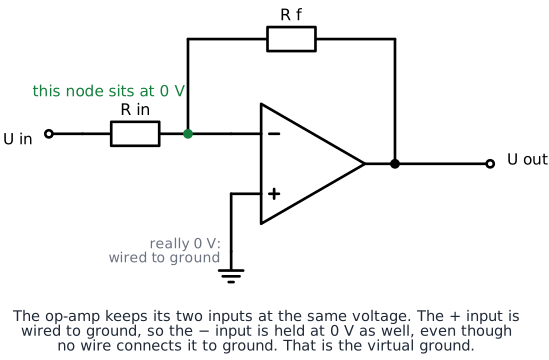
Look at the + input: it is wired to ground, so it sits at 0 V. Rule 2 says the op-amp keeps the − input at the same voltage as the + input. Therefore the − input also sits at 0 V.
But there is no wire from that node to ground. Its voltage is being held at 0 V by the op-amp, which adjusts its output continuously to keep it there. We call it a virtual ground: virtual because the voltage is there but the connection is not.
That is what makes the calculations simple. In the drawing above, the left side of R in has U in on it and the right side sits at 0 V, so the current through it is simply . And because rule 1 says none of that current can flow into the op-amp, all of it has to continue through R f.
The Standard Circuits
Nine circuits, all built with the same op-amp and a handful of resistors. The difference is only where you connect them.
Inverting amplifier
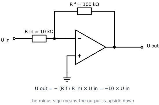
The input goes through a resistor to the inverting input, and the feedback resistor goes from the output back to that same node.
Follow the current, using the virtual ground:
- The node at the − input is at 0 V, so the current through R in is .
- No current enters the op-amp, so exactly that same current flows on through R f.
- That current has to come from the output, so the output sits at .
Put together:
The minus sign means the output is upside down: a positive input gives a negative output. The gain is set purely by the ratio of two resistors, which is the whole point. Two components you can buy for a cent decide what an amplifier with a gain of 200 000 actually does.
Example. R in = 10 kΩ and R f = 100 kΩ gives a gain of −10. An input of 0,2 V produces an output of −2 V.
Non-inverting amplifier
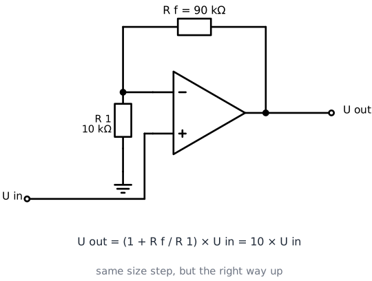
Here the signal goes to the + input, and the feedback network divides the output down to the − input.
Rule 2 says the − input must equal the + input, which is U in. The divider made by R f and R 1 sets what fraction of the output arrives there, and the op-amp adjusts until that fraction equals U in:
Two differences from the inverting version:
- The output is the right way up, no minus sign.
- The gain can never be less than 1, because of that "1 +" in the formula.
Example. R 1 = 10 kΩ and R f = 90 kΩ gives a gain of 10. An input of 0,2 V produces +2 V.
Buffer
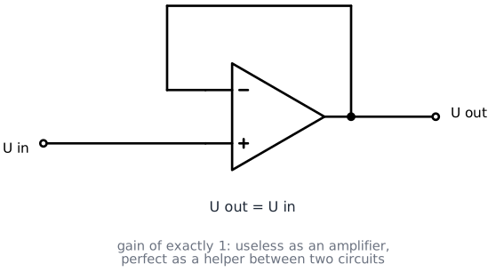
Take the non-inverting amplifier and replace the feedback network with a plain wire. Then R f is 0 and R 1 is infinite, so the gain becomes exactly 1:
An amplifier with a gain of one sounds pointless, and as an amplifier it is. What it does instead is separate two circuits. Its input draws practically no current, and its output can deliver current without its voltage sagging.
Remember the problem at the end of lesson 3: whatever you connect behind an RC filter draws current and shifts its cut-off frequency. Put a buffer in between and the filter no longer notices that anything is connected. This is one of the most used op-amp circuits in the world, and it costs you one component.
Summing amplifier
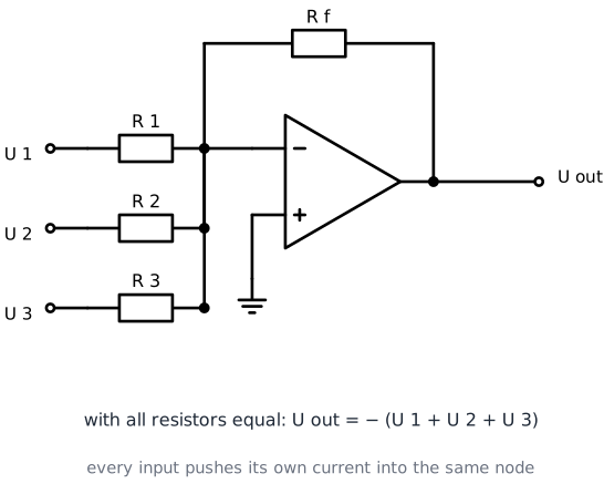
Add a second and a third input resistor to the inverting amplifier, all arriving at the same virtual ground.
Each input pushes its own current into that node, and the node cannot absorb any of it, so all the currents add up and flow together through R f:
If all the resistors have the same value, that collapses to something you can read out loud:
Example. With all resistors at 10 kΩ, inputs of 1 V and 2 V give an output of −3 V.
This is an audio mixer. It is also how you build a simple digital to analogue converter, by feeding it bits weighted with resistors that double each time.
Difference amplifier
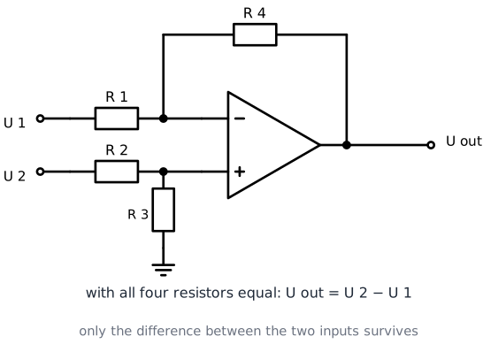
The summing amplifier adds. To subtract, you use both inputs of the op-amp.
With all four resistors equal:
Example. U 2 = 3 V and U 1 = 1 V gives an output of 2 V. Note there is no minus sign in front of the result: the circuit subtracts, it does not invert.
This one matters more than it looks. Any voltage that is present on both inputs at the same time, such as noise picked up by a long sensor cable, is subtracted away and disappears. Only the real difference survives. That is how industrial sensors send their signal down a factory hall without arriving as rubbish.
Adder and subtractor together
Put the two together and you can build any combination of additions and subtractions with weights. Feed the output of a summing amplifier into a difference amplifier and you have a circuit that computes something like in real time, with no processor involved. That is what the "operational" in operational amplifier means: these things were built to do arithmetic, in the analogue computers that came before digital ones.
Integrator and differentiator
Swap one resistor for a capacitor and the circuit stops calculating with values and starts calculating with time.
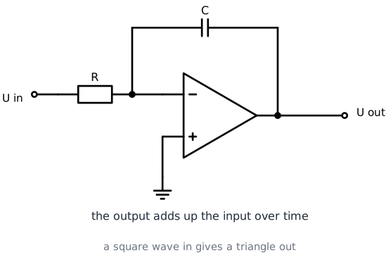
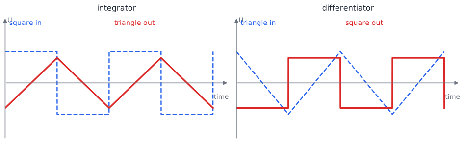
The integrator has a capacitor in the feedback path. The input current charges that capacitor steadily, so the output ramps. It adds the input up over time.
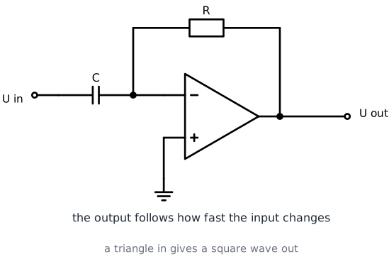
The differentiator has the capacitor at the input instead. A capacitor only passes current while the voltage across it changes, so the output follows how fast the input is changing. A steady input gives zero output.
The two are opposites, and it shows in the waveforms:
Neither works exactly like this in practice
A real integrator drifts: the tiniest DC offset at the input charges the capacitor further and further until the output hits a rail. A resistor across the capacitor fixes it.
A real differentiator amplifies noise, because noise is by definition the fastest changing thing in your signal. A small resistor in series with the input capacitor fixes that one.
Comparator
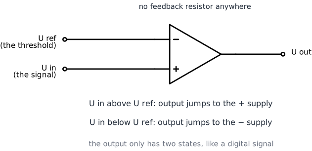
Remove the feedback entirely and rule 2 no longer applies. The op-amp returns to what it always wanted to do: multiply the difference between its inputs by 200 000.
The result is a circuit with only two possible outputs:
- U in above U ref: the output slams to the positive supply
- U in below U ref: the output slams to the negative supply
That is a comparator, and it is the bridge between the analogue and the digital world. On one side a voltage that can be anything, on the other side a signal that is either high or low. A light sensor that switches a lamp on at dusk is a comparator: the LDR divider from lab 1 on one input, an adjustable threshold on the other.
Comparator with hysteresis: the Schmitt trigger
A plain comparator has a problem. Real signals are never clean, and near the threshold the noise on the signal crosses it over and over again. The output then rattles between high and low a dozen times where you wanted one clean switch.
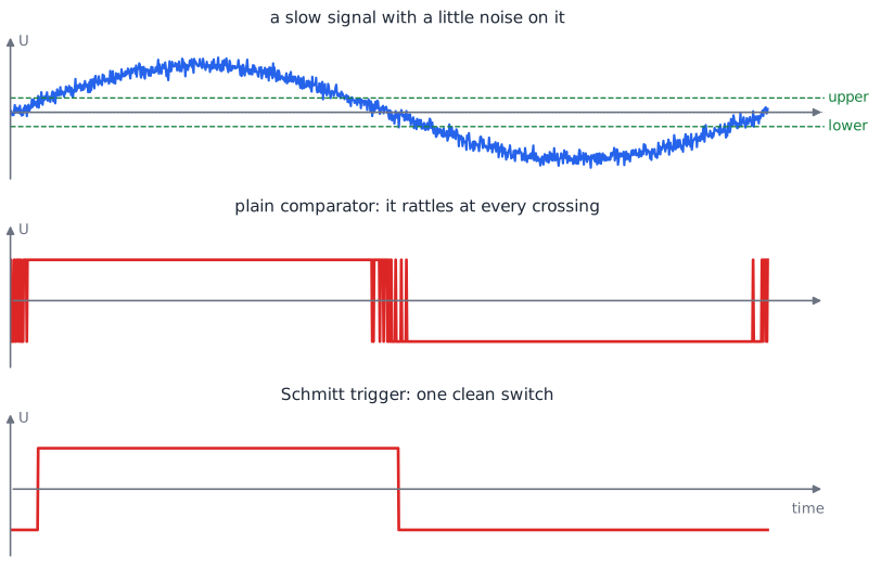
The fix is to give the circuit two thresholds instead of one: a higher one to switch on and a lower one to switch off. Between the two, the output simply does not change its mind. That gap is called hysteresis, and the circuit is a Schmitt trigger.
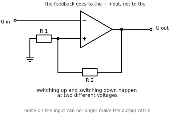
Building it takes one change: the feedback resistor goes to the + input instead of the − input. That is positive feedback, and it makes the circuit reinforce its own decision. Once the output goes high, it drags the threshold up with it, so the input has to fall a lot further before anything switches back.
With R 1 and R 2 and an output that swings to about ±12 V, the two thresholds sit at:
Example. R 1 = 10 kΩ, R 2 = 100 kΩ and an output swing of ±12 V gives thresholds of about ±1,1 V. The signal has to climb above +1,1 V to switch the output up, and then fall below −1,1 V before it switches back down.
You will meet this again in digital electronics. Every input of every logic chip has a Schmitt trigger in it, for exactly this reason.
All of them together
| Circuit | Input goes to | Feedback | Formula |
|---|---|---|---|
| Inverting amplifier | − through R in | R f to − | |
| Non-inverting amplifier | + | R f and R 1 to − | |
| Buffer | + | wire to − | |
| Summing amplifier | − through one R per input | R f to − | with equal resistors |
| Difference amplifier | both, through R | R to − | with equal resistors |
| Integrator | − through R | C to − | the input added up over time |
| Differentiator | − through C | R to − | how fast the input changes |
| Comparator | either | none | + supply or − supply |
| Schmitt trigger | − | R to + | + supply or − supply, with two thresholds |
Filters and Amplifiers Together
Now the last three lessons join up.
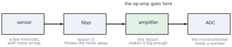
A real sensor gives you a signal that is both dirty and small. A thermocouple delivers a few tens of microvolts per degree. A strain gauge bridge gives millivolts. An ADC input expects volts.
So the chain is almost always the same:
- Filter the signal, with the RC circuits from lesson 3, to throw away the noise that sits outside the frequency band you care about.
- Amplify it, with one of the circuits from this lesson, until it fills the input range of the converter.
- Convert it, and read a number in software.
Two remarks that connect the lessons directly:
- Put a buffer between the filter and whatever comes next. A passive filter changes its own cut-off frequency as soon as it is loaded. A buffer makes the loading disappear.
- Filter first, amplify second. If you amplify first, you amplify the noise as well, and no filter afterwards can undo that.
An active filter does both jobs in one circuit: the RC network sits around the op-amp instead of in front of it. It keeps its cut-off frequency whatever you connect to it, it can amplify at the same time, and it is how filters above first order are built in practice. Calculating one is not part of this course, but you now know both halves of what it is made of.
Try it yourself!
Question 1: An inverting amplifier has R in = 4,7 kΩ and R f = 47 kΩ. What is the gain, and what does an input of 0,5 V give?
Solution
Question 2: You need a gain of exactly 5, the right way up. Which circuit do you use, and which resistors?
Solution
A non-inverting amplifier, because the output must not be inverted.
For example R 1 = 10 kΩ and R f = 40 kΩ. With standard values, 10 kΩ and 39 kΩ gives a gain of 4,9.
Question 3: You build an amplifier with a gain of 100 using an LM741. Up to which frequency does it work?
Solution
Above 10 kHz the gain starts falling, whatever the resistors say.
Question 4: A summing amplifier has three inputs, all with 10 kΩ resistors and R f = 10 kΩ. The inputs are 0,5 V, 1,5 V and 2 V. What is the output?
Solution
Key Takeaways
A bipolar transistor has three layers and three connections: emitter, base and collector, as NPN or PNP. The arrow on the emitter tells you which.
Biasing means setting the DC voltages so the transistor works where you want it. The base to emitter junction needs 0,7 V, just like a diode.
A small base current controls a much larger collector current: , with β typically 100 to 300.
As a switch, a transistor is either in cut-off (open) or in saturation (closed). Drive the base with about five times the calculated minimum current so it saturates properly, and never leave out the base resistor.
That on or off behaviour is the foundation of digital electronics, which is where this course goes next.
An op-amp amplifies the difference between its two inputs by a gain of about 200 000, which is far too much to use directly.
Negative feedback tames it, and gives the two golden rules: no current flows into the inputs, and the output does whatever it takes to make the inputs equal.
The virtual ground follows from those rules: the − input sits at 0 V without being connected to ground, which makes every calculation a matter of Ohm's law.
Gain and bandwidth are a trade-off: gain × bandwidth = 1 MHz for an LM741. The slew rate of 0,5 V/µs limits how fast the output can move, whatever the gain.
The circuit you build is decided by two resistors, not by the op-amp: inverting, non-inverting, buffer, adder, subtractor, integrator, differentiator.
Without feedback the op-amp is a comparator, and with the feedback moved to the + input it is a Schmitt trigger with two thresholds.
The normal chain is sensor, filter, amplifier, converter, and a buffer between the stages stops them from disturbing each other.
Glossary: Key Terms and Abbreviations
These are the new terms from this lesson. The terms from lesson 1, lesson 2 and lesson 3 still apply and are not repeated here.
Active region
The region in which the collector current of a transistor follows the base current multiplied by β. The region used for amplifying.
Base
The control connection of a bipolar transistor, the thin middle layer.
Biasing
Setting the DC voltages on a component so that it works in the region you want.
BJT (Bipolar Junction Transistor)
A transistor built from three layers of doped silicon, as NPN or PNP.
Buffer
An op-amp circuit with a gain of exactly 1, used to separate two circuits so that the second one does not load the first. Also called a voltage follower.
Closed loop gain
The gain of an op-amp circuit once feedback has been added. Set by the resistors, not by the op-amp.
Collector
The connection of a bipolar transistor that collects the charge carriers. Usually the one connected to the load.
Comparator
An op-amp without feedback, whose output is either at the positive or at the negative supply, depending on which input is higher.
Current gain (β or hFE)
How many times larger the collector current is than the base current. Typically 100 to 300 for a small transistor.
Cut-off
The state of a transistor with no base current and therefore no collector current. It behaves like an open switch.
Difference amplifier
An op-amp circuit whose output is the difference between two inputs. Also called a subtractor.
Differentiator
An op-amp circuit whose output follows how fast the input is changing. A capacitor at the input, a resistor in the feedback.
Dual supply
A supply with a positive and a negative voltage relative to ground, for example +12 V and −12 V. Needed when the output has to go below 0 V.
Emitter
The connection of a bipolar transistor that emits the charge carriers. The arrow on the symbol always sits here.
Gain bandwidth product
Gain multiplied by bandwidth, a constant for a given op-amp. 1 MHz for an LM741, so a gain of 10 leaves 100 kHz of bandwidth.
Hysteresis
Using two different thresholds, one for switching up and one for switching down, so that a noisy signal cannot make the output rattle.
Integrator
An op-amp circuit whose output adds up the input over time. A resistor at the input, a capacitor in the feedback.
Inverting amplifier
An op-amp circuit with the signal on the − input and a gain of . The output is upside down.
Inverting input (−)
The op-amp input that drives the output in the opposite direction.
LM741
The classic general purpose op-amp in an 8 pin package, used throughout this lesson.
Negative feedback
Feeding part of the output back to the inverting input, which stabilises the circuit and sets its gain.
Non-inverting amplifier
An op-amp circuit with the signal on the + input and a gain of . The output keeps its sign.
Non-inverting input (+)
The op-amp input that drives the output in the same direction.
NPN
A bipolar transistor with a P layer between two N layers. The one you use by default.
Op-amp (operational amplifier)
An amplifier built from many transistors and sold as one component, with two inputs, one output and a very large gain.
Open loop gain
The gain of an op-amp without any feedback. About 200 000 for an LM741 at DC.
PNP
A bipolar transistor with an N layer between two P layers. Used when the load must sit between the transistor and ground.
Positive feedback
Feeding part of the output back to the non-inverting input, which makes the circuit reinforce its own decision. Used in the Schmitt trigger.
Rail
One of the two supply voltages of an op-amp. An output that is "at the rail" cannot go any further.
Saturation
The state of a transistor that is switched fully on, with only about 0,2 V across it. It behaves like a closed switch.
Schmitt trigger
A comparator with hysteresis, built by feeding the output back to the + input.
Slew rate
The maximum speed at which the output of an op-amp can move, in volts per microsecond. 0,5 V/µs for an LM741.
Summing amplifier
An op-amp circuit that adds several input voltages together. Also called an adder.
Transistor
A three layer semiconductor component that uses a small current or voltage to control a much larger one. Works as a switch or as an amplifier.
Virtual ground
A node that is held at 0 V by the op-amp instead of being wired to ground. It appears at the − input of an inverting circuit whose + input is grounded.
Extra Resources
- Electronics Tutorials: Bipolar Transistor and Transistor as a Switch, with more worked examples of base resistor calculations
- Electronics Tutorials: Operational Amplifiers, the full chapter on every circuit in this lesson
- LM741 datasheet (Texas Instruments), so you can look up the numbers used here yourself
- Falstad circuit simulator, which has all of these circuits ready made under Circuits, Op-Amps. Change a resistor and watch the output change while it runs