
Building Blocks within an Embedded System
In the previous two lessons you worked with binary numbers and logic gates. Logic gates are the foundation of all digital circuits, but they have one significant limitation: their output depends only on the current inputs. The moment the inputs change, the output changes immediately. There is no memory.
Most real systems need memory. A microcontroller needs to remember the last sensor reading. A register needs to hold a value while a calculation is in progress. A traffic light controller needs to know what phase it is in. This requires a different kind of circuit: one that can store state.
This lesson introduces the building blocks that give digital systems memory: latches, flip-flops, and the selection circuits called multiplexers.
Combinatorial vs Sequential logic
All digital circuits belong to one of two categories.
Combinatorial logic systems produce an output that depends only on the current inputs at that moment. Nothing about the past matters. The logic gates you studied in the previous lesson are all combinatorial: feed them the same inputs and you always get the same output, regardless of what happened before.

Sequential logic systems have at least one output fed back to the input. This feedback loop means the output depends not just on the current inputs, but also on the history of past inputs. The system has memory. Because of the feedback, truth tables must account for more variables. These include the current stored state.
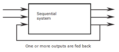
Sequential logic circuits remember conditions and remain in their current state until the next triggering event changes them. The word "sequential" means things happen in a sequence: one after another. The behaviour of the circuit depends on that sequence.
Latches and flip-flops are the fundamental building blocks of sequential systems.
Classification: event, clock, and pulse driven
Sequential circuits can be further categorised by what causes them to change state:
1. Event driven (asynchronous): the circuit changes state immediately when an input signal changes. There is no synchronising clock. These circuits react as fast as the signal changes, but they can be harder to design reliably.
2. Clock driven (synchronous): the circuit only changes state in response to a specific clock signal. All changes are coordinated to happen at the same moment in time. This makes the system predictable and much easier to design and debug. Almost all modern digital systems use synchronous design.
3. Pulse driven: the circuit changes state in response to a short pulse: a brief high or low strobe signal. Used in specific control applications.
SR Latch
The SR latch is the simplest memory element in digital electronics. It has two inputs and two outputs:
- S (Set): brings the output Q to 1
- R (Reset): brings the output Q to 0
- Q: the main output
- /Q: the inverted output (should always be the complement of Q)
An SR latch can be built from two cross-coupled NOR gates (active high inputs) or two cross-coupled NAND gates (active low inputs). The cross-coupling is what creates the feedback and gives the latch its memory.
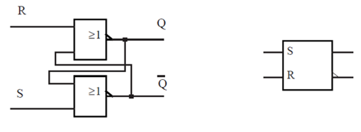
SR latch with NOR gates (active high S and R):
| S | R | Q (next) | Meaning |
|---|---|---|---|
| 0 | 0 | Q (unchanged) | Remember previous state |
| 0 | 1 | 0 | Reset |
| 1 | 0 | 1 | Set |
| 1 | 1 | Forbidden | Both S and R active: not allowed |
The forbidden state occurs when both S and R are 1 at the same time. In that condition, both outputs are forced to the same value, which violates the requirement that Q and /Q are always complementary. This state must be avoided in circuit design.
An SR latch built from NAND gates behaves differently at the input level: the inputs are active low (the latch responds when an input is pulled to 0 rather than 1). The forbidden state now occurs when both inputs are 0 simultaneously.
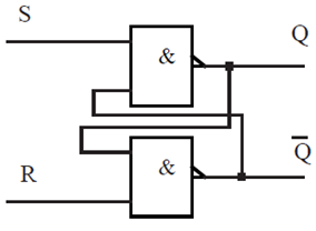
The SR latch has no clock input, so it is an asynchronous (event-driven) device. It reacts immediately whenever S or R changes.

SR Flip-Flop (gated SR latch)
The SR flip-flop is an SR latch with a control input added. This control input, called the Enable or Gate, is implemented by placing an AND gate in series with each of the S and R inputs.
The result is a "gated" latch: S and R can only affect the output when the Enable signal is high. When Enable is low, the latch ignores its S and R inputs entirely, regardless of their state.
This is useful when you want the latch to be "transparent" (responsive) only during a specific window of time. Outside that window, it holds its state regardless of what is happening on the inputs.
| Enable | S | R | Q (next) |
|---|---|---|---|
| 0 | X | X | Q (unchanged) |
| 1 | 0 | 0 | Q (unchanged) |
| 1 | 0 | 1 | 0 (Reset) |
| 1 | 1 | 0 | 1 (Set) |
| 1 | 1 | 1 | Forbidden |
The forbidden state still exists when Enable is high and both S and R are 1. This fundamental limitation led to the development of improved flip-flop types.
How a flip-flop works: a practical example
Let's walk through how an SR flip-flop actually works. We'll start with a scenario, apply a SET command, then a RESET, then another SET to show how the flip-flop remembers and responds.
Starting scenario: Q = 0 (output is OFF). The flip-flop is in Reset state and waiting for commands.
Command 1: SET the flip-flop. We pulse the S input while Enable is high. This triggers the internal feedback loops. The output Q goes from 0 to 1. The flip-flop is now SET and remembers this state.
Command 2: RESET the flip-flop. Now we pulse the R input while Enable is high. This changes the feedback loop. The output Q goes from 1 back to 0. The flip-flop is now RESET.
Command 3: SET again. We pulse S once more. Q goes from 0 to 1 again. This demonstrates that the flip-flop is reusable. It does not "forget" how to respond. Each pulse of S or R triggers a change.
This simple cycle is the foundation of all digital memory. Every bit stored in a microcontroller's RAM, every register that holds a value, every state machine that remembers where it is: all of these are built from flip-flops just like this one, working in concert.
JK Flip-Flop
The JK flip-flop was developed by Jack Kilby (the J and K stand for his initials). It solves the forbidden state problem of the SR flip-flop.
In a JK flip-flop:
- J replaces S (Set)
- K replaces R (Reset)
- The Enable is replaced by a clock input, making the system synchronous
The key improvement: when both J and K are 1 at the same time (the previously forbidden state), the output simply toggles: it flips to the opposite of its current value. There is no forbidden state.
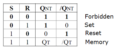
JK flip-flop truth table:
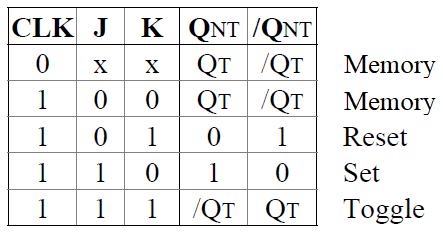
The ↑ symbol means the output only changes on the rising edge of the clock: the moment CLK goes from 0 to 1. Between clock edges, the output is stable. Many JK flip-flops also have asynchronous Set and Reset (PR/preset and CLR/clear) pins that can force the output to a known state independently of the clock.
D Flip-Flop
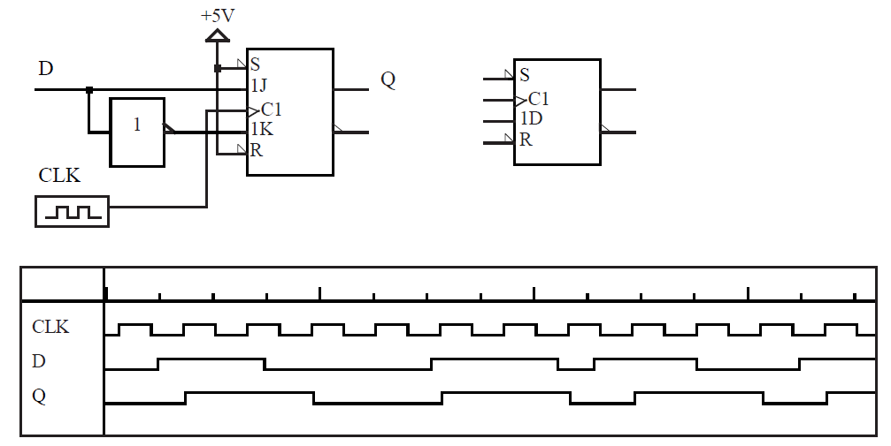
The D flip-flop (Data flip-flop) is the most commonly used flip-flop in modern digital design. It is derived directly from the JK flip-flop by connecting K to the inverse of J. With this modification, the flip-flop has a single data input D.
The rule is beautifully simple: whatever value is on D when the clock rises, that value appears on Q after the rising edge. The flip-flop samples D on the clock edge and holds that value until the next rising edge.
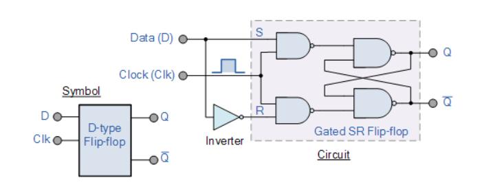
| CLK | D | Q (next) |
|---|---|---|
| ↑ | 0 | 0 |
| ↑ | 1 | 1 |
The timing diagram below shows this behaviour clearly: Q only updates at the moment the clock rises, and then holds that value until the next rising edge. It does not matter what D does in between.
Practical rule
If you want a specific value on Q after the next rising edge of the clock, simply put that value on D beforehand.
The D flip-flop is the fundamental building block of:
- Registers (groups of flip-flops that store a multi-bit value)
- Shift registers (chains of flip-flops where each one feeds the next)
- Counters (circuits that increment or decrement a stored value)
- Memory cells in RAM
In an IoT microcontroller, every register that stores a configuration setting or a sensor reading is ultimately made of D flip-flops.
Multiplexers and Demultiplexers
As digital systems grow in complexity, you need circuits that can route signals. These direct data from one of several sources to a common destination, or from one source to one of several destinations.
Multiplexer (MUX)
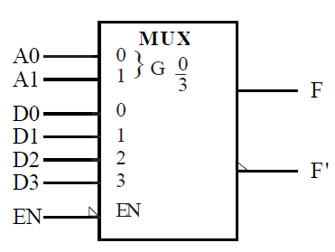
A multiplexer takes multiple data inputs and forwards exactly one of them to the output. The selection is controlled by an address bus: a set of select pins that determine which input is forwarded.
A 4-to-1 multiplexer has:
- 4 data inputs (D0 to D3)
- 2 address/select pins (A0 and A1). Since 2 bits can address 4 channels
- 1 output (F)
- An active-low Enable pin (EN)
| A1 | A0 | Output connected to |
|---|---|---|
| 0 | 0 | D0 |
| 0 | 1 | D1 |
| 1 | 0 | D2 |
| 1 | 1 | D3 |
Think of a multiplexer as a rotary selector switch with a binary control input.
It is useful whenever you need to route one of several signals through a single wire: for example, sharing one ADC channel across multiple sensors.
Demultiplexer (DMUX)
A demultiplexer does the opposite: it takes one input and forwards it to one of several outputs. The select pins again determine which output receives the signal.
A 1-to-4 demultiplexer has:
- 1 data input (D)
- 2 address/select pins (A0 and A1)
- 4 outputs (F0 to F3)
| A1 | A0 | Data sent to |
|---|---|---|
| 0 | 0 | F0 |
| 0 | 1 | F1 |
| 1 | 0 | F2 |
| 1 | 1 | F3 |
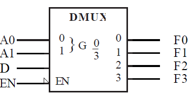
A MUX/DMUX pair together can route a signal through a system: the MUX selects which source to listen to, and the DMUX selects which destination to send it to. Data inputs on analog multiplexers (such as the 74HCT4066 or 74HCT4051) can carry analog signals as well as digital ones: an important tool for routing sensor signals in mixed-signal IoT designs.
Reading the IEC symbol
IEC symbols for multiplexers and demultiplexers follow the same convention as for logic gates, extended with additional notation:
Gmeans gate (AND function): used for the enable pin- A bubble on the enable pin means it is active low
- Address lines are labelled with their significance: A1, A0
{brackets group related pinsF'means the inverted output (complement of F)
Being able to read these symbols in datasheets without the physical chip in front of you is a key skill for working with digital circuits.